 Acer File Extensions |
Acer V55LA Motherboard
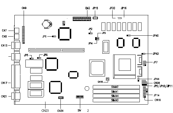
Jumper and Connector Layout

Note - The blackened pin of a jumper represents pin 1.
Specification
The V55LA system has the following features -
- ZIF socket 7 for an Intel Pentium 75/90/100/120/133/150/166/200MHz including MMX.
- Four 72-pin SIMM sockets that support 4/8/16/32-MB 60/70ns fast page mode or EDO SIMMS.
- 256K pipeline-burst second level cache onboard which is not upgradeable.
- 1-MB video memory plus upgrade sockets for a further 1-MB (some systems shipped with the 1-MB upgrade fitted). The chips needed for the upgrade are - 2 of 514260ASL 256Kb x 16 70ns SOJ.
- 128K BIOS which is APM and Year 2000 compliant.
- Two Enhanced IDE interfaces supporting a total of four devices including hard drives and CDROMs.
- External ports.
- PS/2 keyboard and mouse ports.
- Two high-speed (NS16C550 compatible) serial ports.
- One ECP/EPP high-speed parallel port.
- VGA port.
- Onboard chipsets.
- Aladdin III system chipset (equivalent to Intel Triton II).
- ATI Mach64 VT PCI graphics adapter.
- CMD 0646 E-IDE controller.
- SMC 93X I/O controller.
- Plug and Play support.
- Power management features (device standby, global standby).
CPU Jumper Settings
| CPU Freq, | 1 | 2 | 3 | 4 |
|---|---|---|---|---|
| Intel 75 MHz | ON | ON | OFF | OFF |
| Intel 90 MHz | ON | OFF | OFF | OFF |
| Intel 100 MHz | OFF | ON | OFF | OFF |
| Intel 120 MHz | ON | OFF | ON | OFF |
| Intel 133 MHz | OFF | ON | ON | OFF |
| Intel 150 MHz | ON | OFF | ON | ON |
| Intel 166 MHz | OFF | ON | ON | ON |
| Intel 200MHz | OFF | ON | OFF | ON |
| Cyrix/IBM 6x86 P120+ | ON | ON | ON | OFF |
| Cyrix/IBM 6x86 P150+ | ON | OFF | ON | OFF |
| NB For Intel MMX processors set JP7 Open, JP43 and JP44 2-3 | ||||
SW2 Settings
| Switch | Setting | Function |
|---|---|---|
| CPU Clock Frequency Switches 1, 2 | ON, ON ON, OFF OFF, ON | 75/50 MHz 90/60, 120/60, 150/60 MHz 100/66, 133/66, 166/66, 200/66 MHz |
| CPU Frequency Ratio Switches 3, 4 | ON, ON OFF, OFF ON, OFF OFF, ON | Intel M1 K5 5/2 1/1 2/1 3/2 3/1 3/2 2/1 2/1 - 3/1 4/1 - |
| Sound Feature Switch 5 | ON OFF | Onboard sound chip disabled Onboard sound chip enabled |
| Password Security Switch 6 | ON OFF | Password bypass Password check |
Jumper Settings
| Jumper | Setting | Function |
|---|---|---|
| JP1 BIOS Type | 1-2 2-3 | For models with Acer BIOS For models with OEM BIOS |
| JP2 LED Function | 1-2 2-3 | LED for IDE and FDD LED for IDE only |
| JP3, JP4 Second-level Cache | 1-2, 1-2 1-2, 2-3 2-3, 2-3 | 256 KB 512 KB 1 MB |
| JP5 Flash BIOS fn (Intel 28F001 only) | 1-2 2-3 | Allows boot block programming Normal operation |
| JP6 BIOS ROM Type | 1-2 2-3 Open | Flash ROM (28F010) EPROM Block Flash EEPROM (SST 29EE010) |
| JP7 Regulator | Closed Open | For CPUs using one voltage (P54C) For CPUs using two voltages (P55C) |
| JP11 SMM/Reset Switch | 1-2 2-3 3-4 | Supports SMM switch Supports reset switch Functions as additional reset switch conn |
| JP16 Software Shutdown | 1-2 2-3 | UPS enabled UPS disabled |
| JP42 L2 Cache Mode | 1-2 2-3 | Intel or M1 "1+4" mode M1 linear burst mode |
| CPU Voltage JP43 (for I/O) JP44 (for core) | 1-2 2-3 1-2 2-3 | 3.5V 3.3V 2.5V 2.8V |
Connector Functions
| Connector | Function |
|---|---|
| CN3 | Power connector |
| CN5 | USB Connector |
| CN7 | PS/2 keyboard connector |
| CN8 | PS/2 mouse connector |
| CN10 | Diskette drive connector |
| CN11 | IDE connector 2 |
| CN12 | IDE connector 1 |
| CN13 | Serial port 1 |
| CN14 | Serial port 2 |
| CN17 | Parallel port |
| CN18 | CPU fan connector |
| CN21 | Video port |
| CN23 | ATI multimedia connector (AMC) |
| CN30 | Reset switch connector (pins 1-2) |
| JP9 | Hard disk and power LED connector (Fujitsu) |
| JP10 | Hard disk and diskette drive LED connector |
| JP14 | Power-on switch connector (pins 1-2) |
| JP15 | Standby power connector |
| JP30 | External battery connector |
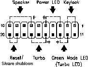
| The multifunction connector CN19 accommodates the front panel connectors for speaker, LEDs, keylock, reset, and turbo. Figure below shows the pin assignments for each connector. |
 |
Memory
Module description : 72pin EDO 60 or 70ns Maximum : 128MB
Video RAM Upgrade
Video Memory can be upgraded from 1MB to 2MB by inserting 2 of 514260ASL 256Kb x 16 70ns SOJ in sockets U3, U4