Acer File Extensions |
Acer A1GX-2 Motherboard
Jumper and Connector Layout
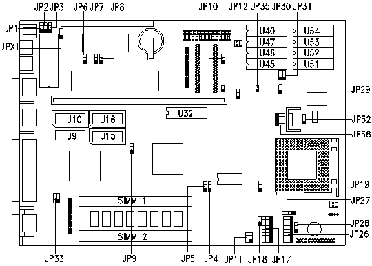
Note - The blackened pin of a jumper represents pin 1.
Overview
- CPU Information:
- Socket: ZIF
- CPU Types: Intel 80486 SX, Intel 80486 SX2, Intel 80486 DX, Intel 80486 DX2, Intel P24T, Intel P24D, Intel P24C, Cyrix, IBM, TI, AMD
- Clockspeeds: 25 MHz, 33 MHz, 40 MHz
- On-Board Memory: 4 MB RAM (non-parity)
- On-Board Video: CL-GD5430 5440/5434
- BIOS Type: Acer Flash
- Bus Type: Riser Card: 3 ISA
- On-Board Controller: Enhanced IDE (M5213N)
- Chipset: ALI
- I/O Ports:
- 2 9-pin Serial (NS16C550)
- 1 25-pin Parallel
- (Bi-directional) (EPP) (ECP)
- Cases: Aspire Desktop
CPU Jumper Settings
| Intel 486 3.3V(P24C) | Intel 486 3.3V WB | Cyrix/IBM/TI DX2 | Cyrix/IBM/TI DX2 | Cyrix DX4/100 | TI DX4/100 | Cyrix 5x86 (M1SC) | AMD DX2 NV8T | |
|---|---|---|---|---|---|---|---|---|
| JP17 | 2-3 | 2-3 | 1-2 | 1-2 | 1-2 | 1-2 | 1st 1-2 6th 2-3 7th 2-3 | 2-3 |
| JP18 | 1-2 | 1-2 | 2-3 | 2-3 | 2-3 | 2-3 | Open | 1-2 |
| JP19 | 2-3 | 1-2 | 1-2 | 1-2 | 1-2 | 2-3 | 1-2 | 2-3 |
| JP26 | 2-3 | 1-2 | 2-3 | 2-3 | 2-3 | 2-3 | 4th 1-2 5th 1-2 6th 2-3 7th 2-3 | 2-3 |
| JP27 | 3-4 | 3-4 | 3-4 | 3-4 | 3-4 | 3-4 | 3-4 | 2-3 |
| JP32 | 1-2 | 1-2 | 1-2 | 2-3 | 1-2 | 1-2 | 1-2 | 1-2 |
| JP36 | 1-2 | 1-2 | 1-2 | 1-2 | 1-2 | 1-2 | 1-2 | 1-2 |
| AMD DX4 NV8T | AMD DX2 NV8B | AMD DX4 NV8B | Enhanced AMD DX2 SV8T(WT) | Enhanced AMD DX4 SV8T(WT) | Enhanced AMD DX2 SV8B(WB) | Enhanced AMD DX4 SV8B(WB) | |
|---|---|---|---|---|---|---|---|
| JP17 | 2-3 | 2-3 | 2-3 | 2-3 | 2-3 | 2-3 | 2-3 |
| JP18 | 2-3 | 1-2 | 2-3 | 2-3 | 2-3 | 1-2 | 1-2 |
| JP19 | 2-3 | 1-2 | 1-2 | 1-2 | 1-2 | 1-2 | 1-2 |
| JP26 | 2-3 | 1-2 | 1-2 | 2-3 | 2-3 | 1-2 | 1-2 |
| JP27 | 3-4 | 2-3 | 3-4 | 2-3 | 3-4 | 2-3 | 3-4 |
| JP32 | 1-2 | 1-2 | 1-2 | 1-2 | 1-2 | 1-2 | 1-2 |
| JP36 | 1-2 | 1-2 | 1-2 | 1-2 | 1-2 | 1-2 | 1-2 |
Jumper Settings
| Jumper | Setting | Function |
|---|---|---|
| JP1 | 1-2 2-3 | OEM BIOS Acer BIOS |
| JP2 | 1-2 2-3 | Enable password check Bypass password |
| JP3 | 1-2 2-3 | MONO/COM1 boot Normal (VGA) |
| JP5 | 2-3 1-2 | Enable onboard memory Disable onboard memory |
| JP6 | 2-3 1-2 | Enable onboard super I/O chip Disable onboard super I/O chip |
| JP7 | 1-2 2-3 | Printer DRQ1 Printer DRQ3 |
| JP8 | 1-2 2-3 | Printer DACK1 Printer DACK3 |
| JP9 | 2-3 1-2 | Enable onboard VGA Disable onboard VGA |
| JP10 | 2-3 1-2 | IDE port 074H, 078H, 07CH IDE port 0F4H, 0F8H, 0FCH |
| JP 11 | 1-4 2-5 3-6 | 25 MHz clock frequency 33 MHz clock frequency 40 MHz clock frequency |
| JP 12 | 2-3 2-3 1-2 | 25 MHz clock frequency 33 MHz clock frequency 40 MHz clock frequency |
| JP28 | 1-2 2-3 | Enable Suspend/Resume button Enable Reset button |
| JP29 | 1-2 2-3 | Disable onboard IDE Enable onboard IDE |
| JP33 | 1-2 2-3 | Feature connector I2C interface |
| JP35 | Open Closed | IDE LED function IDE, FDD, CD-ROM LED functions |
| JPX1 | 1-2 2-3 | Flash ROM EPROM |
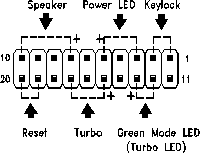
| CN8 accommodates the front panel connectors for speaker, LEDs, keylock, reset, and turbo. Figure 1-3 shows the CN17 pin assignments for each of the front panel connectors. |
Memory
Module Description : 72-Pin, 70ns, Non-Parity Fast Page Mode SIMMS with gold tips. Maximum : 32MB
Video Memory
The system board comes with 1-MB video memory onboard upgradable to 2 MB. Contact Acer to order the video upgrade kit. Note - 800x600x16 million colors is not available when video memory is upgraded to 2 MB on CL-5430 and CL-5440 chipsets.
Cache RAM Upgrade Path
| Size | Data chips | Tag chip | JP30 | JP31 |
|---|---|---|---|---|
| 128K | 4 of 32Kb x 8 (U51 - U54) | 32Kb x 8 (U32) | 1-2* | 1-2* |
| 256K | 8 of 32Kb x 8 (U40,U45-7,U51-4) | 32Kb x 8 (U32) | 2-3 | 2-3 |
Note - Speed in both cases is 15ns for all chips