Acer File Extensions |
Acer A1GX-1 Motherboard
Jumper and Connector Layout
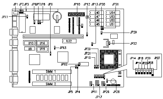
Note - The blackened pin of a jumper represents pin 1.
Overview
The system board has the following major components:
- 486SX, SX2, DX2, or DX4 series CPU
- 4-MB onboard RAM expandable to 36 MB
- Two 72-pin SIMM sockets for memory upgrade
- 128-KB ROM for system BIOS and VGA BIOS
- 120-pin connector for ISA riser card
- System clock/calendar
- Two 9-pin serial ports
- One 25-pin Centronics parallel port
- PS/2-compatible keyboard and mouse interface
- 512-KB or 1-MB DRAM for onboard local bus VGA interface; expandable to 2 MB
- Embedded fixed disk interface
- Upgradable cache memory (128-KB or 256-KB)
- Optional enhanced IDE interface
CPU Jumper Settings
| Intel 486/P24C AMD NV8T/NV8B | 486 WB/ P24D | Enhanced AMD DX2 SV8T(WT) | Enhanced AMD DX4 SV8T(WT) | Enhanced AMD DX2 SV8B(WB) | Enhanced AMD DX4 SV8B(WB) | Cyrix/ IBM/TI DX2 | Cyrix/ IBM/TI DX2 | Cyrix/IBM DX4/100 | Cyrix/ IBM 5x86 (M1SC) | Pentium OverDrive P24T | |
|---|---|---|---|---|---|---|---|---|---|---|---|
| JPX2 | 2-3 | 2-3 | 2-3 | 2-3 | 2-3 | 2-3 | 2-3 | 2-3 | 2-3 | 2-3 | 2-3 |
| JP13 | 2-3 | 2-3 | 2-3 | 2-3 | 2-3 | 2-3 | 2-3 | 2-3 | 2-3 | 2-3 | 2-3 |
| JP14 | 2-3 | 2-3 | 2-3 | 2-3 | 2-3 | 2-3 | Open | Open | Open | 2-3 | 2-3 |
| JP15 | 2-3 | 2-3 | 2-3 | 2-3 | 2-3 | 2-3 | 1-2 | 1-2 | 1-2 | Open | 2-3 |
| JP17 | 2-3 | 2-3 | 2-3 | 2-3 | 2-3 | 2-3 | 1-2 | 1-2 | 1-2 | 1st 1-2 | 2-3 |
| JP18 | 2-3 | 2-3 | 2-3 | 2-3 | 1-2 | 1-2 | 2-3 | 2-3 | 2-3 | Open | 2-3 |
| JP19 | 2-3 | 1-2 | 1-2 | 1-2 | 1-2 | 1-2 | 1-2 | 1-2 | 1-2 | 1-2 | 1-2 |
| JP20 JP21 JP23 | 2-3 | 2-3 | 2-3 | 2-3 | 2-3 | 2-3 | 1-2 | 1-2 | 1-2 | 2-3 | 2-3 |
| JP22 JP26 | 2-3 | 1-2 | 2-3 | 2-3 | 1-2 | 1-2 | 2-3 | 2-3 | 2-3 | 2-3 4th 1-2 | 1-2 |
| JP25 | 2-3 | 2-3 | 2-3 | 2-3 | 2-3 | 2-3 | 2-3 | 2-3 | 2-3 | Open | 2-3 |
| JP27 | 3-4 | 3-4 | 2-3 | 3-4 | 2-3 | 3-4 | 3-4 | 3-4 | 3-4 | 3-4 | 1-2 |
| JP32 | 1-2 | 1-2 | 1-2 | 1-2 | 1-2 | 1-2 | 1-2 | 2-3 | 2-3 | 1-2 | 1-2 |
Jumper Settings
| Jumper | Setting | Function |
|---|---|---|
| JP1 | 1-2 2-3* | OEM BIOS Acer BIOS |
| JP2 | 1-2 2-3* | Enable password check Bypass password |
| JP3 | 1-2 2-3* | COM1 boot Normal boot |
| JP4, JP5 | 1-2, 2-3* 2-3, 1-2 1-2, 1-2 | Enable onboard memory (4MB) Enable onboard memory (8MB) Disable onboard memory (4MB/8MB) |
| JP6 | 1-2 2-3* | Disable onboard super I/O chip Enable onboard super I/O chip |
| JP7 | 2-3* 1-2 | Printer DRQ3 Printer DRQ1 |
| JP8 | 1-2 2-3* | Printer DACK1 Printer DACK3 |
| JP9 | 1-2 2-3* | Disable onboard VGA Enable onboard VGA |
| JP10 | 1-2 2-3* | IDE port 0F4H, 0F8H, 0FCH IDE port 074H, 078H, 07CH |
| JP11 | 1-5 2-6 3-7 | 25 MHz 33 MHz 40 MHz (not recommended) |
| JP28 | 1-2 2-3* | Enable Suspend/Resume button Enable Reset button |
| JP29 | 1-2 2-3* | Disable the onboard IDE Enable the onboard IDE |
| JPX1 | 1-2 2-3* | Flash ROM EPROM |
Connector Functions
| Connector | Feature |
|---|---|
| CN1 | VGA Feature connector |
| CN2 | Diskette drive connector |
| CN11 | Reserved |
| CN4 | Secondary IDE Connector |
| CN5 | Primary IDE Connector |
| CN6 | CPU Fan connector |
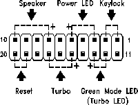
| CN8 | Multifunction connector |
| CN8 accommodates the front panel connectors for speaker, LEDs, keylock, reset, and turbo. Figure 1-3 shows the CN17 pin assignments for each of the front panel connectors. |
Memory
The system board has two 72-pin SIMM sockets that accept 4-MB, 8-MB, or 16-MB Non-Parity Fast Page Mode memory modules with 70 ns (or less) DRAM speed. Maximum : 32MB
Cache RAM Upgrade Path
| Size | Data chips | Tag chip | JP30, JP31 |
|---|---|---|---|
| 128K | 4 of 32Kb x 8 (U51-U54) | 32Kb x 8 (U32) | 1-2* |
| 256K | 8 of 32Kb x 8 (U40,U45-47,U51-54) | 32Kb x 8 (U32) | 2-3 |